- 您现在的位置:买卖IC网 > Sheet目录317 > C8051F380-TB (Silicon Laboratories Inc)DEV KIT FOR C8051F38X
�� �
�
�C8051F380/1/2/3/4/5/6/7/C�
�14.5.� Multiplexed� and� Non-multiplexed� Selection�
�The� External� Memory� Interface� is� capable� of� acting� in� a� Multiplexed� mode� or� a� Non-multiplexed� mode,�
�depending� on� the� state� of� the� EMD2� (EMI0CF.4)� bit.�
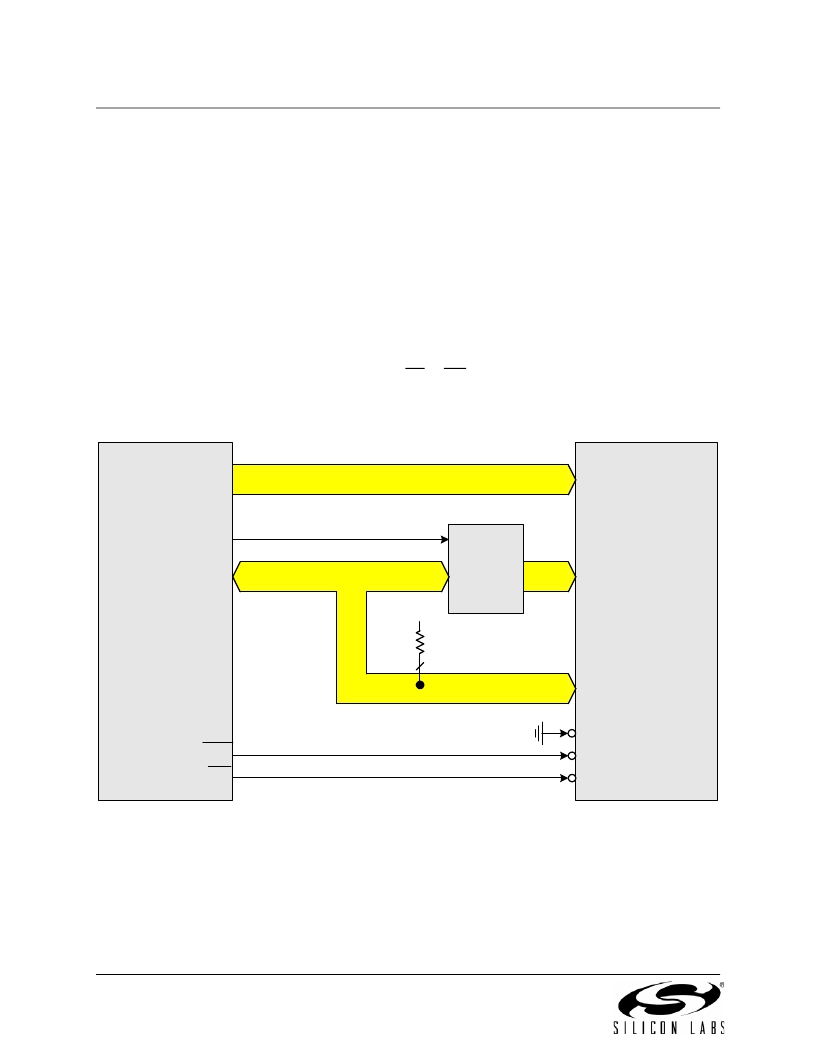
�14.5.1.� Multiplexed� Configuration�
�In� Multiplexed� mode,� the� Data� Bus� and� the� lower� 8-bits� of� the� Address� Bus� share� the� same� Port� pins:�
�AD[7:0].� In� this� mode,� an� external� latch� (74HC373� or� equivalent� logic� gate)� is� used� to� hold� the� lower� 8-bits�
�of� the� RAM� address.� The� external� latch� is� controlled� by� the� ALE� (Address� Latch� Enable)� signal,� which� is�
�driven� by� the� External� Memory� Interface� logic.� An� example� of� a� Multiplexed� Configuration� is� shown� in�
��In� Multiplexed� mode,� the� external� MOVX� operation� can� be� broken� into� two� phases� delineated� by� the� state�
�of� the� ALE� signal.� During� the� first� phase,� ALE� is� high� and� the� lower� 8-bits� of� the� Address� Bus� are� pre-�
�sented� to� AD[7:0].� During� this� phase,� the� address� latch� is� configured� such� that� the� ‘Q’� outputs� reflect� the�
�states� of� the� ‘D’� inputs.� When� ALE� falls,� signaling� the� beginning� of� the� second� phase,� the� address� latch�
�outputs� remain� fixed� and� are� no� longer� dependent� on� the� latch� inputs.� Later� in� the� second� phase,� the� Data�
�Bus� controls� the� state� of� the� AD[7:0]� port� at� the� time� RD� or� WR� is� asserted.�
�See� Section� “14.7.2.� Multiplexed� Mode”� on� page� 107� for� more� information.�
�A[15:8]�
�ADDRESS� BUS�
�74HC373�
�A[15:8]�
�E�
�M�
�ALE�
�AD[7:0]�
�ADDRESS/DATA� BUS�
�V� DD�
�G�
�D�
�Q�
�A[7:0]�
�64K� X� 8�
�I�
�F�
�8�
�(Optional)�
�SRAM�
�I/O[7:0]�
�CE�
�WR�
�RD�
�WE�
�OE�
�Figure� 14.2.� Multiplexed� Configuration� Example�
�14.5.2.� Non-multiplexed� Configuration�
�In� Non-multiplexed� mode,� the� Data� Bus� and� the� Address� Bus� pins� are� not� shared.� An� example� of� a�
�Non-multiplexed� Configuration� is� shown� in� Figure� 14.3.� See� Section� “14.7.1.� Non-multiplexed� Mode”� on�
��98�
�Rev.� 1.4�
�发布紧急采购,3分钟左右您将得到回复。
相关PDF资料
C8051F912DK
KIT DEV FOR C8051F91X/C8051F90X
C8051F930-TB
BOARD TARGET/PROTO W/C8051F930
C8051T610DB24
DAUGHTER BOARD T610 24QFN SOCKET
C8051T630DB20
BOARD SOCKET DAUGHTER 20-QFN
CAN-100
BOARD EVAL RS232 100QFP
CANADAPT28
KIT ADAPTER CANDEMOBOARD 28PLCC
CAT24AA01WI-GT3
IC EEPROM SERIAL 1KB I2C 8SOIC
CAT24AA02WI-G
IC EEPROM SERIAL 2KB I2C 8SOIC
相关代理商/技术参数
C8051F381
制造商:SILABS 制造商全称:SILABS 功能描述:USB DRIVER CUSTOMIZATION
C8051F381-GM
功能描述:8位微控制器 -MCU USB-64K-Flash
RoHS:否 制造商:Silicon Labs 核心:8051 处理器系列:C8051F39x 数据总线宽度:8 bit 最大时钟频率:50 MHz 程序存储器大小:16 KB 数据 RAM 大小:1 KB 片上 ADC:Yes 工作电源电压:1.8 V to 3.6 V 工作温度范围:- 40 C to + 105 C 封装 / 箱体:QFN-20 安装风格:SMD/SMT
C8051F381-GMR
功能描述:8位微控制器 -MCU USB-Flash-64k-ADC RoHS:否 制造商:Silicon Labs 核心:8051 处理器系列:C8051F39x 数据总线宽度:8 bit 最大时钟频率:50 MHz 程序存储器大小:16 KB 数据 RAM 大小:1 KB 片上 ADC:Yes 工作电源电压:1.8 V to 3.6 V 工作温度范围:- 40 C to + 105 C 封装 / 箱体:QFN-20 安装风格:SMD/SMT
C8051F381-GQ
功能描述:8位微控制器 -MCU USB-64K-Flash
RoHS:否 制造商:Silicon Labs 核心:8051 处理器系列:C8051F39x 数据总线宽度:8 bit 最大时钟频率:50 MHz 程序存储器大小:16 KB 数据 RAM 大小:1 KB 片上 ADC:Yes 工作电源电压:1.8 V to 3.6 V 工作温度范围:- 40 C to + 105 C 封装 / 箱体:QFN-20 安装风格:SMD/SMT
C8051F381-GQR
功能描述:8位微控制器 -MCU USB-Flash-64k-ADC RoHS:否 制造商:Silicon Labs 核心:8051 处理器系列:C8051F39x 数据总线宽度:8 bit 最大时钟频率:50 MHz 程序存储器大小:16 KB 数据 RAM 大小:1 KB 片上 ADC:Yes 工作电源电压:1.8 V to 3.6 V 工作温度范围:- 40 C to + 105 C 封装 / 箱体:QFN-20 安装风格:SMD/SMT
C8051F382
制造商:SILABS 制造商全称:SILABS 功能描述:USB DRIVER CUSTOMIZATION
C8051F382-GQ
功能描述:8位微控制器 -MCU USB-Flash-32k-ADC
RoHS:否 制造商:Silicon Labs 核心:8051 处理器系列:C8051F39x 数据总线宽度:8 bit 最大时钟频率:50 MHz 程序存储器大小:16 KB 数据 RAM 大小:1 KB 片上 ADC:Yes 工作电源电压:1.8 V to 3.6 V 工作温度范围:- 40 C to + 105 C 封装 / 箱体:QFN-20 安装风格:SMD/SMT
C8051F382-GQR
功能描述:8位微控制器 -MCU USB-Flash-32k-ADC RoHS:否 制造商:Silicon Labs 核心:8051 处理器系列:C8051F39x 数据总线宽度:8 bit 最大时钟频率:50 MHz 程序存储器大小:16 KB 数据 RAM 大小:1 KB 片上 ADC:Yes 工作电源电压:1.8 V to 3.6 V 工作温度范围:- 40 C to + 105 C 封装 / 箱体:QFN-20 安装风格:SMD/SMT